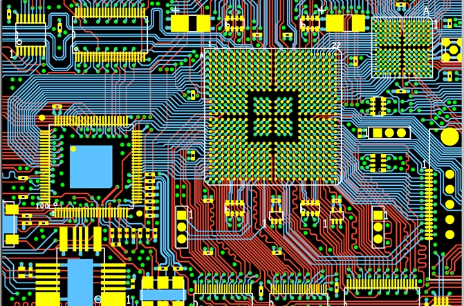
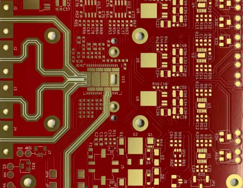
737 DDR5 PCB Layout Guidelines: The Design Rules You Must Follow Pcb routing guidelines for ddr4 memory devices and impedance
If you are searching about PCB Layout Guidelines For High Speed Applications - HardwareBee you've visit to the right page. We have 25 Pictures about PCB Layout Guidelines For High Speed Applications - HardwareBee like pcb design layout guidelines Pcb layout guidelines for design, PCB Design Rules and Tips and also Rectifier PCB Layout: Best Practices and Design Tips – Hillman Curtis. Here it is:
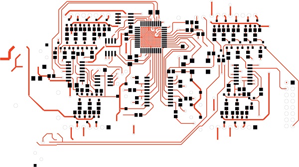
PCB Layout Guidelines For High Speed Applications - HardwareBee
 hardwarebee.com
PCB Layout Guidelines For High Speed Applications - HardwareBee
Pcb Design Guidelines Mechanical Layer Eurocircuits Eurocircuits Images
 www.tpsearchtool.com
Pcb Design Guidelines Mechanical Layer Eurocircuits Eurocircuits Images
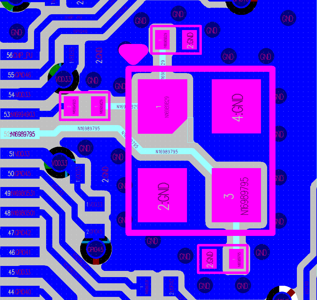
Grounding Pcb Crystal Layout Electrical Engineering S - Vrogue.co
 www.vrogue.co
Grounding Pcb Crystal Layout Electrical Engineering S - vrogue.co
Component Placement In PCB Design & Assembly | Sierra Circuits
 www.protoexpress.com
Component Placement in PCB Design & Assembly | Sierra Circuits
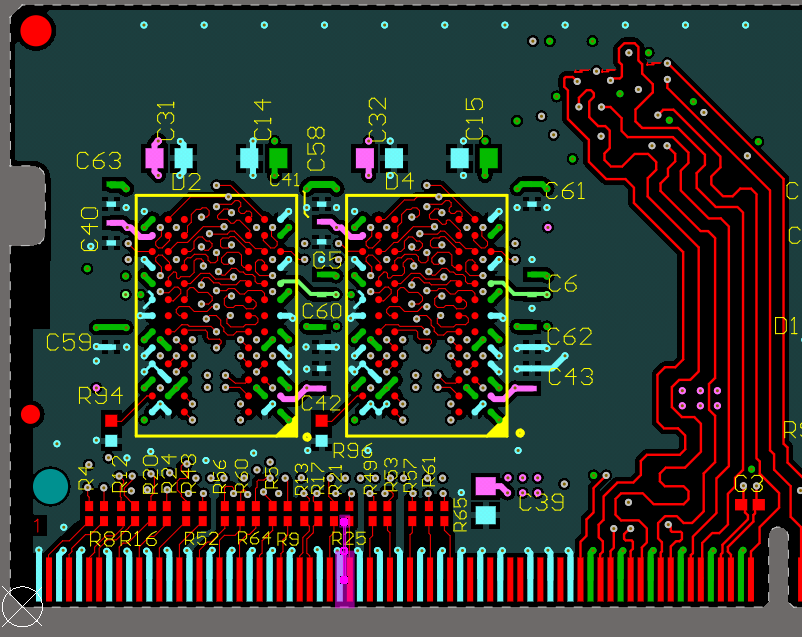
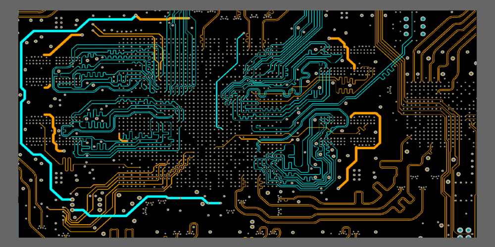
Pcb Routing Guidelines - Design Talk
 design.udlvirtual.edu.pe
Pcb Routing Guidelines - Design Talk
Pcb Design Layout Guidelines Pcb Layout Guidelines For Design
 pcbways.pages.dev
pcb design layout guidelines Pcb layout guidelines for design
PCB Layout Guidelines And Considerations
 www.microcontrollertips.com
PCB layout guidelines and considerations
Top PCB Design Guidelines Every PCB Designer Needs To Know | Altium
 www.pinterest.co.uk
Top PCB Design Guidelines Every PCB Designer Needs to Know | Altium ...
Switched-Mode Power Supply PCB Design Guidelines | Altium
 resources.altium.com
Switched-Mode Power Supply PCB Design Guidelines | Altium
Antenna Design And RF Layout Guidelines You Must Know - RayPCB
 www.raypcb.com
Antenna Design and RF Layout Guidelines You Must Know - RayPCB
Pcb Design - PCB Layout For Crystal Resonator (STM32) - Electrical
 electronics.stackexchange.com
pcb design - PCB layout for crystal resonator (STM32) - Electrical ...
PCB Design Best Practices And Layout Guidelines | Cadence
 resources.pcb.cadence.com
PCB Design Best Practices and Layout Guidelines | Cadence
Equalizer Circuit Diagram Pcb Layout
 www.circuitdiagram.co
Equalizer Circuit Diagram Pcb Layout
Reparator Credential Dumnezeu Pcb Design Guidelines Releu Alb Ca
 cristor.dz
Reparator Credential Dumnezeu pcb design guidelines releu alb ca ...
PCB Design Rules
 www.build-electronic-circuits.com
PCB Design Rules
Pcb Design Differential Impedance Of Lvds Rules And T - Vrogue.co
 www.vrogue.co
Pcb Design Differential Impedance Of Lvds Rules And T - vrogue.co
Getting Started With RF PCB Layout Guidelines
 www.hemeixinpcb.com
Getting Started With RF PCB Layout Guidelines
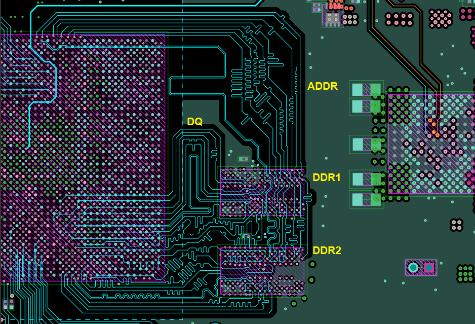
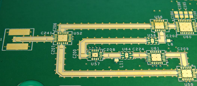
Memory Interfaces(DDR4, DDR5, LPDDR4x)Layout Design Guidelines With
 www.raceelacademy.com
Memory interfaces(DDR4, DDR5, LPDDR4x)Layout design guidelines with ...
PCB Routing Guidelines For DDR4 Memory Devices And Impedance | Blog
 resources.altium.com
PCB Routing Guidelines for DDR4 Memory Devices and Impedance | Blog ...
Ten Golden Rules Of PCB Design & Its Guidelines - AES
 absolutepcbassembly.com
Ten Golden Rules of PCB Design & its Guidelines - AES
PCB Design Rules And Tips
 www.6pcb.com
PCB Design Rules and Tips
Rectifier PCB Layout: Best Practices And Design Tips – Hillman Curtis
 hillmancurtis.com
Rectifier PCB Layout: Best Practices and Design Tips – Hillman Curtis ...
PCB Layout Guidelines For USB Type-C
PCB Layout Guidelines for USB Type-C
Rf Pcb Design Guidelines Outlet Clearance | Brunofuga.adv.br
 brunofuga.adv.br
Rf Pcb Design Guidelines Outlet Clearance | brunofuga.adv.br
Switched-Mode Power Supply PCB Design Guidelines | Altium
 resources.altium.com
Switched-Mode Power Supply PCB Design Guidelines | Altium
Getting started with rf pcb layout guidelines. pcb layout guidelines and considerations. Pcb design rules and tips